- 您现在的位置:买卖IC网 > Sheet目录489 > NTHD2110TT1G (ON Semiconductor)MOSFET P-CH 12V 4.5A CHIPFET
NTHD2110T
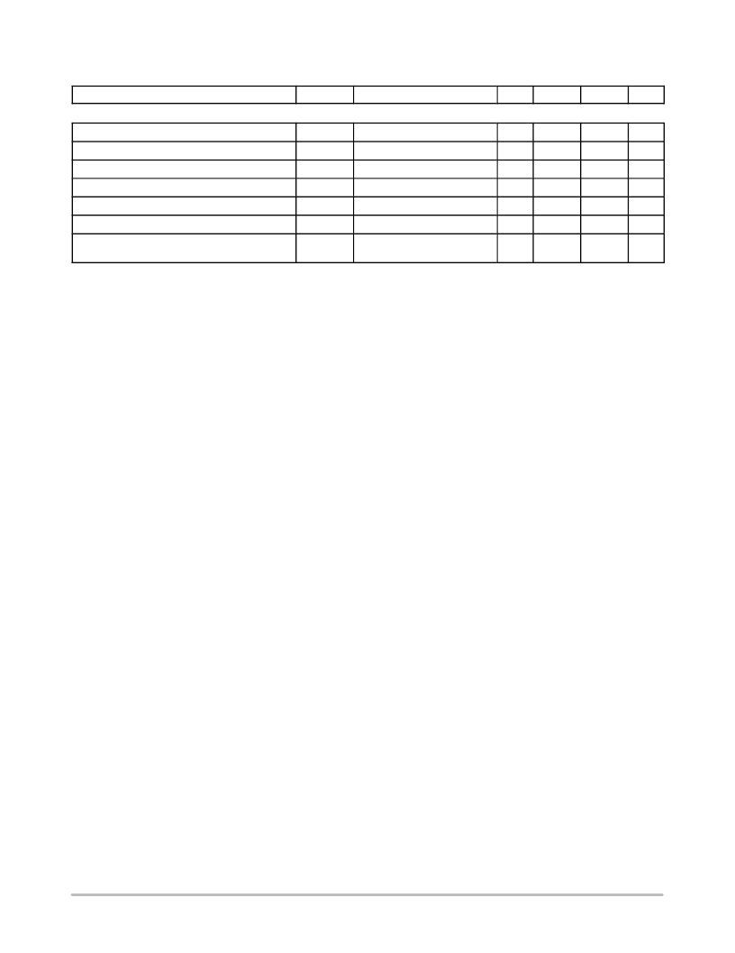
ELECTRICAL CHARACTERISTICS (T J = 25 ° C unless otherwise noted)
Characteristic
Symbol
Test Condition
Min
Typ
Max
Unit
TVS DIODE
Reverse Working Voltage (Note 8)
V RWM
12
V
Breakdown Voltage (Note 9)
Reverse Leakage Current
Clamping Voltage (Note 10)
Clamping Voltage (Note 10)
Maximum Peak Pulse Current (Note 10)
Capacitance
V BR
I R
V C
V C
I PP
CJ
I T = 1 mA
V RWM = 12 V
I PP = 1 A (8 x 20 m s Waveform)
I PP = 5 A (8 x 20 m s Waveform)
8 x 20 m s Waveform
V R = 0 V, f = 1 MHz
14.5
0.6
15.7
10
15.7
19.1
6.2
60
V
nA
V
V
A
pF
(Anode-to-GND)
8. TVS devices are normally selected according to the working peak reverse voltage (V RWM ), which should be equal or greater than the DC
or continuous peak operating voltage level.
9. V BR is measured at pulse test current I T .
10. Pulse waveform per Figure 11.
http://onsemi.com
3
发布紧急采购,3分钟左右您将得到回复。
相关PDF资料
NTHD3100CT3G
MOSFET N/P-CH COMPL 20V CHIPFET
NTHD3101FT3G
MOSFET P-CH 20V 3.2A CHIPFET
NTHD3102CT1G
MOSFET N/P-CH COMPL 20V CHIPFET
NTHD3133PFT3G
MOSFET P-CH SGL 20V CHIPFET
NTHD4102PT3G
MOSFET P-CH DUAL 20V CHIPFET
NTHD4401PT3G
MOSFET 2P-CH 20V 2.1A CHIPFET
NTHD4502NT1
MOSFET N-CHAN DUAL 30V CHIPFET
NTHD4508NT1G
MOSFET 2N-CH 20V 3.1A CHIPFET
相关代理商/技术参数
NTHD3100C
制造商:ONSEMI 制造商全称:ON Semiconductor 功能描述:Power MOSFET 20 V, +3.9 A /−4.4 A, Complementary ChipFET
NTHD3100CT1
功能描述:MOSFET 20V +3.9A/-4.4A RoHS:否 制造商:STMicroelectronics 晶体管极性:N-Channel 汲极/源极击穿电压:650 V 闸/源击穿电压:25 V 漏极连续电流:130 A 电阻汲极/源极 RDS(导通):0.014 Ohms 配置:Single 最大工作温度: 安装风格:Through Hole 封装 / 箱体:Max247 封装:Tube
NTHD3100CT1G
功能描述:MOSFET 20V +3.9A/-4.4A Complementary RoHS:否 制造商:STMicroelectronics 晶体管极性:N-Channel 汲极/源极击穿电压:650 V 闸/源击穿电压:25 V 漏极连续电流:130 A 电阻汲极/源极 RDS(导通):0.014 Ohms 配置:Single 最大工作温度: 安装风格:Through Hole 封装 / 箱体:Max247 封装:Tube
NTHD3100CT3
功能描述:MOSFET 20V +3.9A/-4.4A RoHS:否 制造商:STMicroelectronics 晶体管极性:N-Channel 汲极/源极击穿电压:650 V 闸/源击穿电压:25 V 漏极连续电流:130 A 电阻汲极/源极 RDS(导通):0.014 Ohms 配置:Single 最大工作温度: 安装风格:Through Hole 封装 / 箱体:Max247 封装:Tube
NTHD3100CT3G
功能描述:MOSFET 20V +3.9A/-4.4A Complementary RoHS:否 制造商:STMicroelectronics 晶体管极性:N-Channel 汲极/源极击穿电压:650 V 闸/源击穿电压:25 V 漏极连续电流:130 A 电阻汲极/源极 RDS(导通):0.014 Ohms 配置:Single 最大工作温度: 安装风格:Through Hole 封装 / 箱体:Max247 封装:Tube
NTHD3100F
制造商:ONSEMI 制造商全称:ON Semiconductor 功能描述:Typical Uses for FETKY Devices
NTHD3101F
制造商:ONSEMI 制造商全称:ON Semiconductor 功能描述:Power MOSFET and Schottky Diode
NTHD3101FT1
功能描述:MOSFET -20V -4.4A P-Channel RoHS:否 制造商:STMicroelectronics 晶体管极性:N-Channel 汲极/源极击穿电压:650 V 闸/源击穿电压:25 V 漏极连续电流:130 A 电阻汲极/源极 RDS(导通):0.014 Ohms 配置:Single 最大工作温度: 安装风格:Through Hole 封装 / 箱体:Max247 封装:Tube
